At IMID 2022 held from August 24th to the 26th, Semiconductor Energy Laboratory (SEL) announced that it has developed a 5,291ppi micro OLED display for AR/VR that integrates Si CMOS and OSFET. 
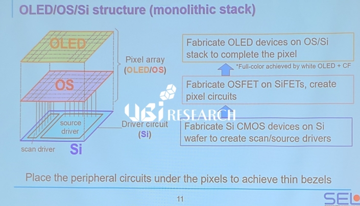
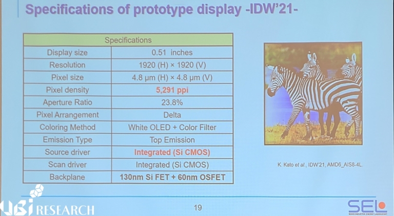
<OLED, OS, Si structure/SEL> According to SEL’sannouncement, two problems arise when manufacturing an OLED display with high pixel density by integrating the existing Si FET. The first is that the source/gate drivers are located outside the display area, which increases the bezel width. A thin bezel width is a prerequisite for a decent AR/VR device size. The second issue is the high mobility of Si FETs and the balance between pixels. In order to apply Si FET to Micro OLED, it is necessary to reduce the transistor size while suppressing the increase in current. In order to solve these problems, SEL announced that it has manufactured an OLED micro-display prototype that integrates Si CMOS and OSFET. SEL states that, “The mobility of OSFETs is not as high as Si FETs, but it is sufficient to drive OLED devices. Through the OLED/OS/Si structure in which OS (OSFET) and OLED are combined on CMOS, the width of the bezel area can be reduced by up to 40%. In addition, in the characteristic evaluation of OSFETs, it was possible to implement deep black and drive a low rate of fire, and the good distribution in a channel length of 200 nm and a breakdown voltage of about 20 V made it suitable for high voltage OLED driving of white-tandem OLED devices.” The size of the 5,291ppi micro OLED display announced by SEL is 0.51 inches, the resolution is 1920×1920, and the pixel size is 4.8×4.8 μm. The backplane is a combined structure of 130 nm Si FET and 60 nm OSFET. 
<5,291ppi Micro OLED display specification/ SEL> |