Special Report
QNED Structure and Manufacturing Technology Analysis Report
₩2,500,000
May 25, 2020
PDF(61P)Introduce
UBI Research published a report analyzing Samsung Display’s 41 published patents for QNED (quantum dot nanorod LED).
Samsung Display is developing QNED as the next-generation display business. Reports on the QNED structure have already been issued through various channels, but the substance of the QNED has not been released.
This report contains directions for the development of QNED technology, including QNED pixel structure and nanorod LED alignment principles analyzed from published patent content. In addition, a manufacturing process constructed based on the structure depicted in the patent was included.
Contents
1. QNED Overview
1.1 Next-generation Large-size Display Structure Comparison
1.2 QNED Structure
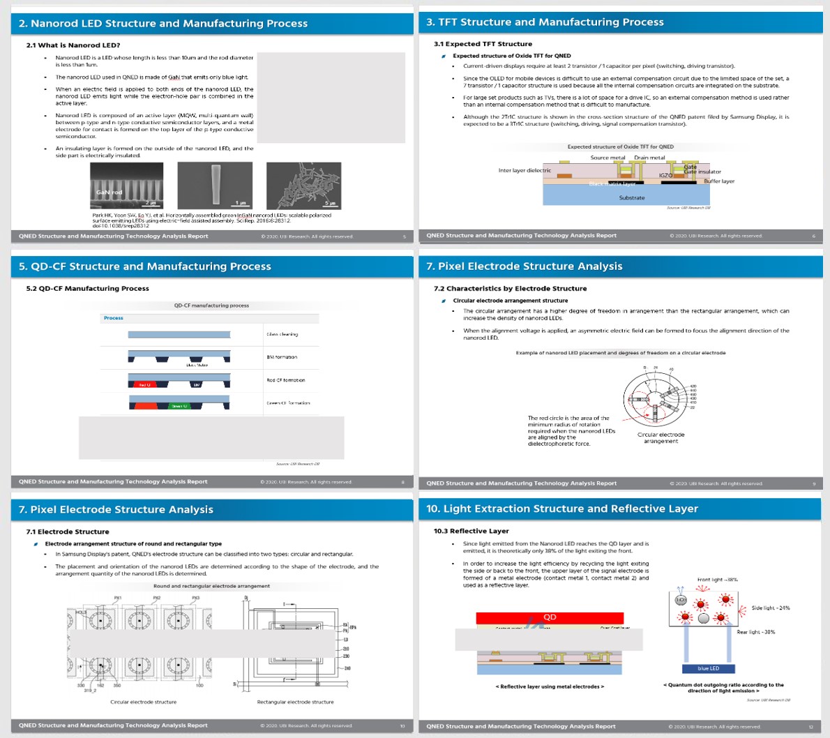
2. Nanorod LED Structure and Manufacturing Process
2.1 What is Nanorod LED?
2.2 Nanorod LED Manufacturing Process
3. TFT Structure and Manufacturing Process
3.1 Expected TFT Structure
3.2 TFT Manufacturing Process
4. Pixel Structure and Manufacturing Process
4.1 Pixel Cross Section Structure
4.2 Pixel Manufacturing Process
5. QD-CF Structure and Manufacturing Process
5.1 Color Conversion Layer Structure
5.2 QD-CF Manufacturing Process
6. Assembly
6.1 Panel assembly
6.2 Panel Assembly Manufacturing Process
7. Electrode Structure Analysis
7.1 Electrode Structure
7.2 Characteristics by Electrode Structure
7.3 Alignment Electrode Gap Adjustment
8. Nanorod LED Alignment Technology
8.1 Alignment Principle
8.2 Nanorod LED Alignment Sequence
8.3 Nanorod LED Alignment Waveform
8.4 Dipole Strengthening Technology
9. Nanorod LED Count control Technology
9.1 Dam Structure for Ink Level Adjustment
9.2 Characteristics by Dam Structure
9.3 Dam Structure for Nanorod LED Alignment
10. Light Extraction Structure and Reflective Layer
10.1 Light Extraction Structure
10.2 Lens Method
10.3 Reflective Layer
11. QNED Development History Analysis
11.1 Nanorod LED Separation Technology Change
11.2 Nanorod LED Insulation Structure Change
11.3 Electrode Structure Changes
11.4 Pixel Structure Change
12. The Meaning of QNED Development and Its Impact on the Display Industry
Report Sample
Previous Report Status
Related Products
-

QNED Technical Analysis Report
₩6,000,000November 12, 2020
PDF(164P)This report consists of a detailed analysis of 94 patents filed by Samsung Display in relation to QNED, which were released by the second week of October 2020. In the first half of last year, QNED was analyzed as 41 patents, and there was a difference of about 6 months in the additional patents, but surprisingly technological progress was confirmed. The backplane of QNED is 7T2C TFT, and it was found that the oscillator for aligning the nano-rod LED and the transistor for repair are arranged together. The QNED circuit was configured similar to the TFT structure used in OLED for mobile devices. Since QNED is also a current driven device, it seems that precise control is required. Large OLED uses 3T1C structure.
-

QNED Technology Maturity Analysis Report
₩6,000,000June 22, 2021
PDF(271P)The reality of QNED (quantum dot nano-rod LED) that Samsung Display is preparing as a next-generation display has become clear.
As a result of analyzing 160 patents applied by Samsung Display, it was confirmed that the structure constituting the QNED has already been completed, and that the only remaining task is to keep the number of nano-rod LEDs arranged in the light-emitting pixel constant.
The number of aligned nano-rod LEDs per pixel, which determines the yield and image quality of QNED, is determined by the distribution of LEDs in the ink, the number of LEDs injected into the pixel, and the alignment ratio of the injected LEDs. -

2026 Analysis Report on China’s OLED Supply Chain Management
₩0May 1, 2026
PDF(103P)The newly published ‘2026 Analysis Report on China’s OLED Supply Chain Management’ is the first in the industry to organize, at a glance, the customer landscape and business stage of a wide range of OLED materials, components, and equipment companies in China. It is expected to serve as a practical guideline for global companies seeking to enter China’s steadily expanding OLED market.
The way panel makers build and maintain their supply chain management is a key determinant of their technological competitiveness. SCM is critically important not only for panel manufacturers, but also for materials, components, and equipment suppliers. To succeed in business, companies must clearly understand who their customers are, who their competitors are, and, for new entrants, how the existing market structure is already laid out.
There is a common denominator behind Samsung Display’s position as the global leader in panel technology and Apple’s strong leadership in the OLED smartphone business: SCM. The biggest reason Chinese panel makers and set manufacturers have not been able to scale as rapidly in OLED as they did in LCD is the supply chain. It is not possible to free-ride on the SCM networks that Samsung Display and Apple have already built.


