

Special Report
AMOLED Manufacturing Process Report Ver.4
₩4,000,000
January 5, 2022
Introduction
The AMOLED manufacturing process report analyzes the structure and manufacturing process by dividing AMOLED into small, medium-sized, and
large-area. They also schematically design the inspection process of small and medium-sized AMOLED, so each company can understand the overall structure and core processes of AMOLED.
In the currently published AMOLED process report ver.4, the QD-OLED structure and process were updated, and the structure and process were added based on the decapsulated LTPO TFT applied to the Galaxy Note21.
This report is a must-read report for not only panel makers but also equipment, components, and materials makers to understand the AMOLED manufacturing process.
Contents
1. AMOLED Structure
1.1 Panel Structure for Mobile Device
1.2 Panel Structure for TV
1.3 Substrate
1.4 TFT
1.5 Color Filter
1.6 OLED Pixel
1.7 Encapsulation
1.8 Touch Screen Panel
1.9 Module
2. TFT Manufacturing Process
2.1 LTPS TFT Manufacturing Equipment Layout
2.2 LTPS TFT Basic Manufacturing Process
2.3 SDC LTPS TFT Manufacturing Process
2.4 Oxide TFT Basic Manufacturing Process
2.5 LGD OLED TV’s Oxide TFT Manufacturing Process
2.6 TFT Inspection and Measurement Process
3. OLED Pixel and Encapsulation Manufacturing Process
3.1 OLED Pixel and Encapsulation Manufacturing Equipment Layout
3.2 Small Size Rigid OLED Manufacturing Process
3.3 Manufacturing Process of Flexible OLED for Mobile Device
3.4 WRGB OLED Manufacturing Process
3.5 Solution Process OLED Manufacturing Process
3.6 OLED Pixel Inspection and Measurement Process
3.7 Encapsulation Inspection and Measurement Process
4. Cell Manufacturing Process
4.1 Cell Manufacturing Equipment Layout
4.2 Small Size Rigid OLED Manufacturing Process
4.3 Small Size Flexible OLED Manufacturing Process
4.4 Flexible On-cell Touch Manufacturing Process
4.5 Cell Inspection and Measurement Process
5. Module Manufacturing Process
5.1 Equipment Layout for Module Manufacturing
5.2 Small Size Rigid OLED Manufacturing Process
5.3 Small Size Flexible OLED Manufacturing Process
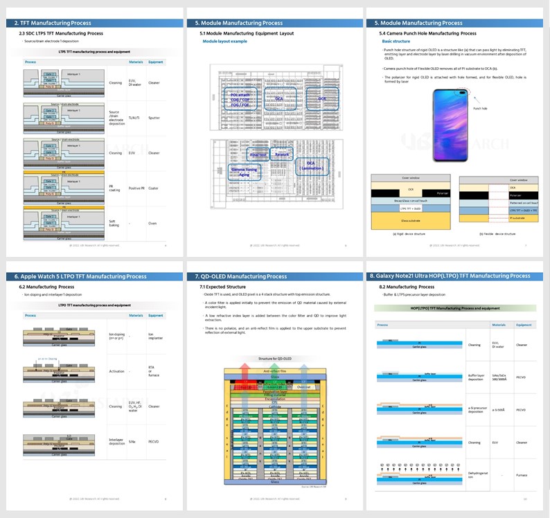
5.4 Camera Punch Hole Manufacturing Process
5.5 Foldable OLED Module Manufacturing Process
5.6 Module Inspection and Measurement Process
6. Apple Watch 5 LTPO TFT Manufacturing Process
6.1 Structure
6.2 Manufacturing Process
7. QD-OLED Manufacturing Process
7.1 Expected Structure
7.2 Oxide TFT Manufacturing Process
7.3 Encapsulation Manufacturing Process
7.4 QD Color Filer Manufacturing Process
7.5 Total
8. Galaxy Note21 Ultra HOP(LTPO) TFT Manufacturing Process
8.1 Structure
8.2 Manufacturing Process
Report Sample
Previous Report Status
Related Products
-

AMOLED Manufacturing Process Report Ver.5
₩4,000,000January 19, 2023
The AMOLED manufacturing process report contains the structure, manufacturing process, and inspection process of small and medium-large OLEDs for each layer, from the substrate to the module.
In the AMOLED Process Report Ver.5 published this time, the structure of foldable OLED, the light emitting structure history of WRGB OLED and QD-OLED, and the structure and process of a color filter on encapsulation(COE) have been newly added or updated.
This report is a must-read for understanding the AMOLED manufacturing process of display-related companies. -

Small Sized AMOLED Manufacturing Process Report Ver. 6
₩4,000,000March 8, 2024
The Small Sized AMOLED Manufacturing Process Report covers the manufacturing process for each type of TFT, including LTPS and LTPO TFT, as well as OLED structure and manufacturing process, inspection process, and module manufacturing process.
In this small sized AMOLED manufacturing process report, the Galaxy Z Fold5 structure and module process have been updated for the small OLED manufacturing process. In addition, the eLEAP process and SEL’s photolithography process, which are photolithography OLED processes that have attracted great attention as high-resolution microdisplay OLED manufacturing processes, have been newly added or updated.
This report is a must-read for display companies to understand the AMOLED manufacturing process from TFT substrate to module manufacturing. -

Middle and Large Sized AMOLED Manufacturing Process Report Ver. 6
₩4,000,000March 8, 2024
This report covers the manufacturing process of each type of TFT, including LTPO and Oxide TFT, as well as the structure and cell manufacturing process of OLEDs.
The MLA (micro lens array) formation process for enhancing the brightness of WOLED TVs and the encapsulation process for QD-OLED TVs have been added to the medium and large AMOLED manufacturing process report. Also newly added or updated are the Oxide TFT process with a reduced number of masks, and the eLEAP process and SEL’s photolithography process, which are photolithography OLED processes that have recently attracted great attention as new 8th generation substrate OLED manufacturing processes.
This report will be a must-read for display companies to understand the AMOLED manufacturing process from TFT substrate to cell manufacturing.