Special Report
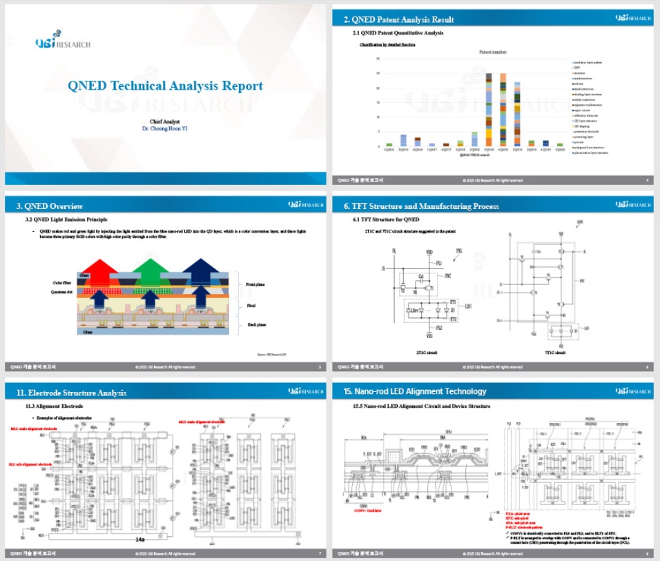
QNED Technical Analysis Report
₩6,000,000
November 12, 2020
PDF(164P)Introduce
This report consists of a detailed analysis of 94 patents filed by Samsung Display in relation to QNED, which were released by the second week of October 2020. In the first half of last year, QNED was analyzed as 41 patents, and there was a difference of about 6 months in the additional patents, but surprisingly technological progress was confirmed.
The backplane of QNED is 7T2C TFT, and it was found that the oscillator for aligning the nano-rod LED and the transistor for repair are arranged together. The QNED circuit was configured similar to the TFT structure used in OLED for mobile devices. Since QNED is also a current driven device, it seems that precise control is required. Large OLED uses 3T1C structure.
Among the additionally confirmed contents, the most remarkable one is the built-in alignment transistor (oscillator). Nano-rod LEDs are dropped onto the panel in ink state and aligned by dielectrophoretic force by the electric field applied to the panel. At this time, the number of nano-rod LEDs and the pixel yield are determined according to the alignment waveform. Oscillator technology has never been used in displays.
A concern among experts regarding QNED is yield. Since about 10 to 20 nano-rod LEDs that are supposed to be arranged in a pixel are all electrically connected, a short circuit may occur in the pixel due to self-defect or misalignment of the nano-rod LED. In order to solve this problem, Samsung Display has placed a series/parallel hybrid connection wiring structure and a repair transistor. The backplane manufacturing technology is much more complex than the previously expected structure, but it has been confirmed that it has a built-in technology that can secure a yield directly related to business feasibility.
This report contains patents related to solvents for nano-rod LED inks. Viscosity control is a key technology for the conditions necessary to disperse the nano-rod LED and for good alignment after spraying. Samsung Display was using a breakthrough technology that could change the viscosity of the solvent in the process.
In addition, the configuration of the inkjet equipment was described in detail. The inkjet printer system consisted of a unit that injects nano-rod LED ink, a module that checks the position and amount of the injected ink, and a unit that senses the number of aligned nano-rod LEDs. The inkjet printer was equipped with a technology capable of correcting the ink viscosity and quantity, inkjet head position by analyzing the results evaluated in each process and feeding back to the inkjet unit.
Samsung Display started filing for QNED patents in 2016. The technology development period is only 4 years, but the level of technology confirmed as a patent filed until 2019 is expected to have no problem with investment in mass production equipment in 2021.
If you are a display expert, you can see that the quality of QNED technology is close to mass production as analyzed in this report.
Contents
Outline
1.Samsung Display’s Large Display Business Direction
1.1 Current Status of Large OLED Business for TV
1.2 Withdrawal of LCD Business and Promotion of QD-OLED Business
1.3 QD-OLED Structure and Manufacturing Technology
1.4 QD-OLED vs WRGB OLED
1.5 QNED Appearance
2.QNED Patent Analysis Result
2.1 QNED Patent Quantitative Analysis
2.2 QNED Core Technology and Related Items
3.QNED Overview
3.1 QNED Structure
3.2 QNED Light Emission Principle
3.3 Nano-rod LED
3.4 Nano-rod LED Alignment Principle
4.Nano-rod LED Structure and Manufacturing Process
4.1 Nano-rod LED Structure
4.2 Nano-rod LED Manufacturing Process
4.3 Nano-rod LED Damage Prevention
5.Nano-rod LED Ink
5.1 Nano-rod LED Solvent
5.2 Dispersant
5.3 Photodegradable Functional Groups
5.4 Device Orientation Functional Groups
6.TFT Structure and Manufacturing Process
6.1 TFT Structure for QNED
6.2 TFT Manufacturing Process
7.Pixel Structure and Manufacturing Process
7.1 Pixel Structure
7.2 Pixel Manufacturing Process
8.QD-CF Structure and Manufacturing Process
8.1 Why Use QD-CF
8.2 QD-CF Structure
8.3 QD-CF Manufacturing Process
8.4 Other QD-CF Structures
9.Assembly
9.1 Panel Structure
9.2 Panel Assembly Process
10.Circuit Structure
10.1 Circuit for QNED
10.2 Driving Circuit
10.3 Wiring Circuit
11.Electrode Structure Analysis
11.1 Electrode Type
11.2 Main Electrode
11.3 Alignment Electrode
11.4 Contact Electrode
11.5 Floating Electrode
11.6 Reflective Electrode
11.7 Efficient Electrode Arrangement Structure
12. Insulation Layer Structure Analysis
12.1 Insulation Layer Type and Role
12.2 Alignment Function Insulation Layer Type
12.3 Alignment Function Insulation Layer Thickness and Number of Alignments
13.Separation Wall Structure Analysis
13.1 Function of Separation Wall
13.2 Separation Wall Type
14.Bank Structure Analysis
14.1 Bank Structure and Function
15.Nano-rod LED Alignment Technology
15.1 Nano-rod LED Ink and Alignment Process
15.2 Nano-rod LED Alignment Waveform
15.3 Nano-rod LED Alignment Circuit
15.4 Nano-rod LED Alignment Circuit Process
15.5 Nano-rod LED Alignment Circuit and Device Structure
15.6 Nano-rod LED Alignment Enhancement Technology
16.Optical Efficiency Improvement Technology
16.1 Light Extraction Technology
16.2 light Extraction Lens
16.3 Reflection Layer
16.4 Reflection Pattern
16.5 Shading Layer
16.6 High-efficiency Nano-rod LED Structure
16.7 Other Nano-rod LED Arrangement Structure
17.Repair Technology and Yield Improvement
17.1 Pixel Defect
17.2 Repair Transistor
17.3 Laser Repair
17.4 Conductive Pattern for Repair
17.5 Connection Pattern for Repair
18.Inkjet Equipment
18.1 Inkjet Equipment Composition
18.2 Inkjet Printer Unit
18.3 Sensing Unit
18.4 Electric Field Application Module
19.7T2C TFT Structure and Process
19.1 7T2C TFT and pixel Circuit Structure
19.2 7T2C TFT and Pixel Plane Structure
19.3 7T2C TFT and Pixel Cross-sectional Structure
19.4 7T2C TFT and Pixel Manufacturing Process
Report Sample
Previous Report Status
Related Products
-

QNED Technology Maturity Analysis Report
₩6,000,000June 22, 2021
PDF(271P)The reality of QNED (quantum dot nano-rod LED) that Samsung Display is preparing as a next-generation display has become clear.
As a result of analyzing 160 patents applied by Samsung Display, it was confirmed that the structure constituting the QNED has already been completed, and that the only remaining task is to keep the number of nano-rod LEDs arranged in the light-emitting pixel constant.
The number of aligned nano-rod LEDs per pixel, which determines the yield and image quality of QNED, is determined by the distribution of LEDs in the ink, the number of LEDs injected into the pixel, and the alignment ratio of the injected LEDs. -

2025 Automotive Display Technology and Industry Trends Analysis Report
₩0February 18, 2025
PDF(217P)The automotive industry is undergoing rapid transformation beyond mere mechanical innovation, entering the era of Software-Defined Vehicles (SDVs). As autonomous driving technology and electric vehicle advancements accelerate, cars are evolving from simple transportation tools into smart devices centered around user interaction.
-

QNED Structure and Manufacturing Technology Analysis Report
₩2,500,000May 25, 2020
PDF(61P)UBI Research published a report analyzing Samsung Display’s 41 published patents for QNED (quantum dot nanorod LED). Samsung Display is developing QNED as the next-generation display business. Reports on the QNED structure have already been issued through various channels, but the substance of the QNED has not been released. This report contains directions for the development of QNED technology, including QNED pixel structure and nanorod LED alignment principles analyzed from published patent content. In addition, a manufacturing process constructed based on the structure depicted in the patent was included.


